- 您现在的位置:买卖IC网 > Sheet目录3827 > PIC16F877A-I/P (Microchip Technology)IC MCU FLASH 8KX14 EE 40DIP
PIC16F87XA
DS39582B-page 58
2003 Microchip Technology Inc.
6.1
Timer1 Operation in Timer Mode
Timer mode is selected by clearing the TMR1CS
(T1CON<1>) bit. In this mode, the input clock to the
timer is FOSC/4. The synchronize control bit, T1SYNC
(T1CON<2>), has no effect since the internal clock is
always in sync.
6.2
Timer1 Counter Operation
Timer1 may operate in either a Synchronous, or an
Asynchronous mode, depending on the setting of the
TMR1CS bit.
When Timer1 is being incremented via an external
source, increments occur on a rising edge. After Timer1
is enabled in Counter mode, the module must first have
a falling edge before the counter begins to increment.
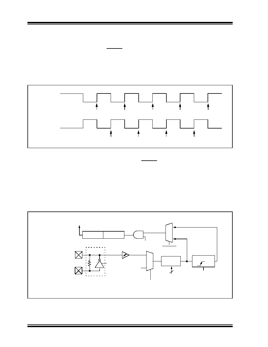
FIGURE 6-1:
TIMER1 INCREMENTING EDGE
6.3
Timer1 Operation in Synchronized
Counter Mode
Counter mode is selected by setting bit TMR1CS. In
this mode, the timer increments on every rising edge of
clock
input on pin
RC1/T1OSI/CCP2 when
bit
T1OSCEN is set, or on pin RC0/T1OSO/T1CKI when
bit T1OSCEN is cleared.
If T1SYNC is cleared, then the external clock input is
synchronized with internal phase clocks. The synchro-
nization is done after the prescaler stage. The
prescaler stage is an asynchronous ripple counter.
In this configuration, during Sleep mode, Timer1 will not
increment even if the external clock is present since the
synchronization circuit is shut-off. The prescaler,
however, will continue to increment.
FIGURE 6-2:
TIMER1 BLOCK DIAGRAM
T1CKI
(Default High)
T1CKI
(Default Low)
Note: Arrows indicate counter increments.
TMR1H
TMR1L
T1OSC
T1SYNC
TMR1CS
T1CKPS1:T1CKPS0
Q Clock
T1OSCEN
Enable
Oscillator(1)
FOSC/4
Internal
Clock
TMR1ON
On/Off
Prescaler
1, 2, 4, 8
Synchronize
det
1
0
1
Synchronized
Clock Input
2
RC0/T1OSO/T1CKI
RC1/T1OSI/CCP2(2)
Note 1: When the T1OSCEN bit is cleared, the inverter is turned off. This eliminates power drain.
Set Flag bit
TMR1IF on
Overflow
TMR1
发布紧急采购,3分钟左右您将得到回复。
相关PDF资料
MP2-HS240-51
CONN SHROUD 2-FB 240POS 5ROW
DSPIC33FJ64MC506-I/PT
IC DSPIC MCU/DSP 64K 64TQFP
DSPIC33FJ128MC802-I/SO
IC DSPIC MCU/DSP 128K 28SOIC
PIC18LF4331-I/P
IC PIC MCU FLASH 4KX16 40DIP
DSPIC33FJ128GP306-I/PT
IC DSPIC MCU/DSP 128K 64TQFP
PIC24HJ128GP306-I/PT
IC PIC MCU FLASH 128KB 64TQFP
PIC16F873-20/SO
IC MCU FLASH 4KX14 EE 28SOIC
PIC18F4431-I/P
IC PIC MCU FLASH 8KX16 40DIP
相关代理商/技术参数
PIC16F877A-I/P
制造商:Microchip Technology Inc 功能描述:IC 8BIT FLASH MCU 16F877 DIP40
PIC16F877A-I/PG
功能描述:8位微控制器 -MCU 14KB 368 RAM 33 I/O RoHS:否 制造商:Silicon Labs 核心:8051 处理器系列:C8051F39x 数据总线宽度:8 bit 最大时钟频率:50 MHz 程序存储器大小:16 KB 数据 RAM 大小:1 KB 片上 ADC:Yes 工作电源电压:1.8 V to 3.6 V 工作温度范围:- 40 C to + 105 C 封装 / 箱体:QFN-20 安装风格:SMD/SMT
PIC16F877A-I/PT
功能描述:8位微控制器 -MCU 14KB 368 RAM 33 I/O RoHS:否 制造商:Silicon Labs 核心:8051 处理器系列:C8051F39x 数据总线宽度:8 bit 最大时钟频率:50 MHz 程序存储器大小:16 KB 数据 RAM 大小:1 KB 片上 ADC:Yes 工作电源电压:1.8 V to 3.6 V 工作温度范围:- 40 C to + 105 C 封装 / 箱体:QFN-20 安装风格:SMD/SMT
PIC16F877A-I/PT
制造商:Microchip Technology Inc 功能描述:8BIT FLASH MCU SMD 16F877 TQFP44
PIC16F877A-I/PTG
功能描述:8位微控制器 -MCU 14KB 368 RAM 33 I/O RoHS:否 制造商:Silicon Labs 核心:8051 处理器系列:C8051F39x 数据总线宽度:8 bit 最大时钟频率:50 MHz 程序存储器大小:16 KB 数据 RAM 大小:1 KB 片上 ADC:Yes 工作电源电压:1.8 V to 3.6 V 工作温度范围:- 40 C to + 105 C 封装 / 箱体:QFN-20 安装风格:SMD/SMT
PIC16F877AIL
制造商:Microchip Technology Inc 功能描述:
PIC16F877AIP
制造商:Microchip Technology Inc 功能描述:
PIC16F877AIPT
制造商:Microchip Technology Inc 功能描述: